TP Series SiPM

TP Series SiPM


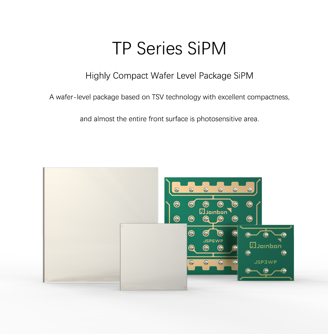
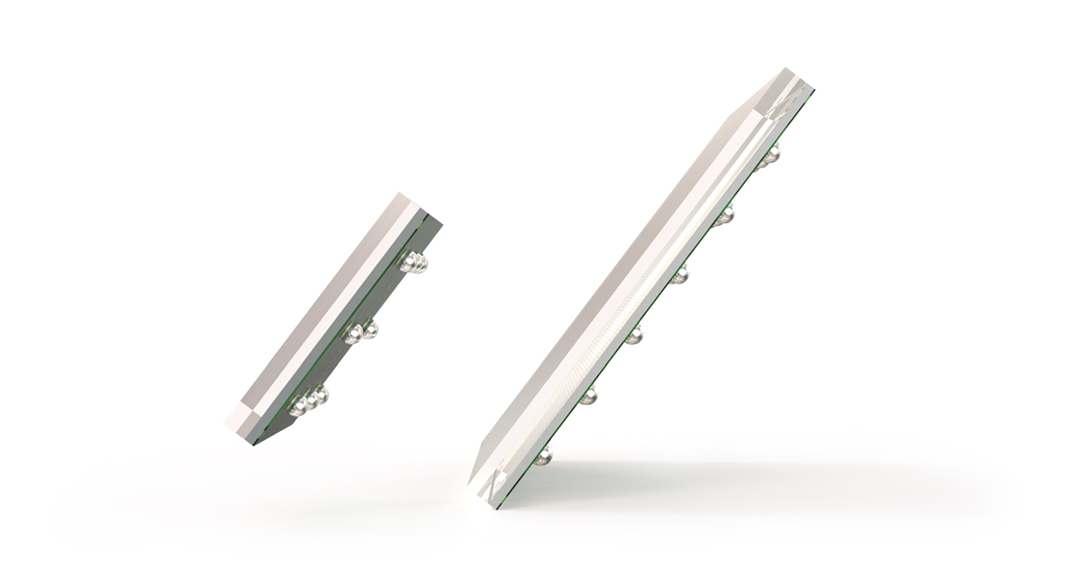
Highly Compact Wafer Level Package SiPM

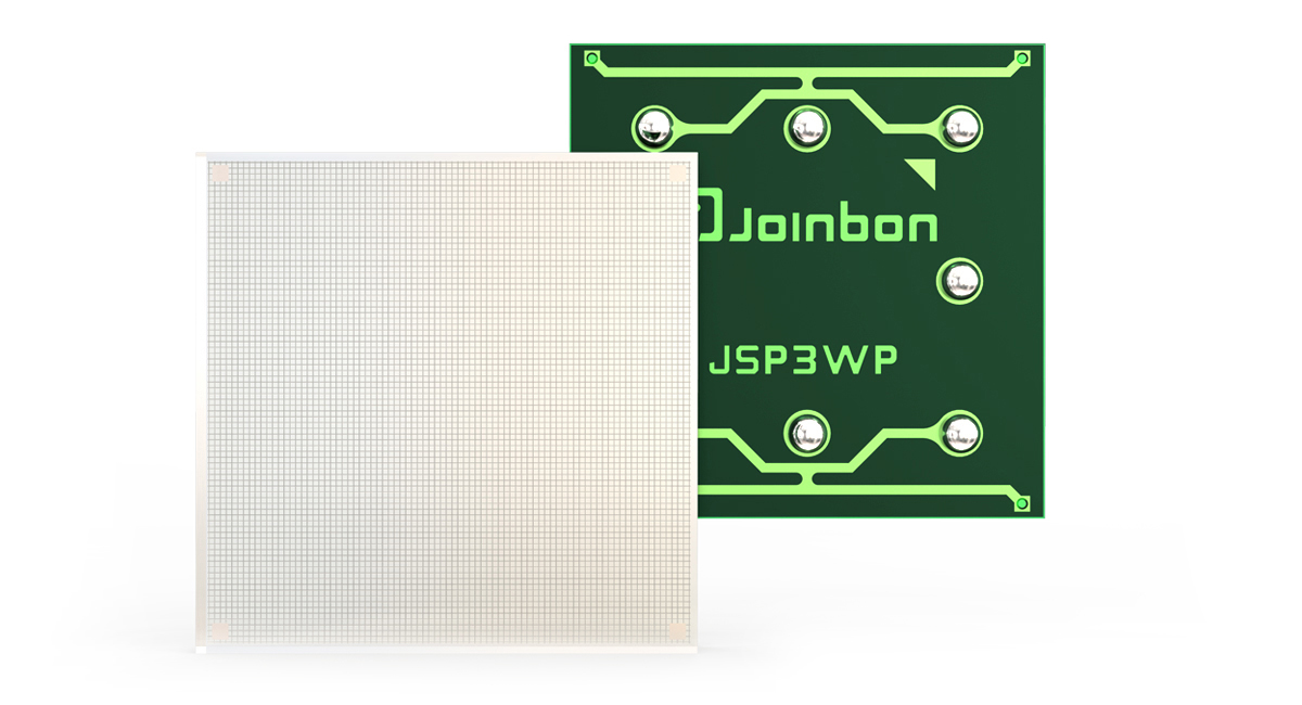
A wafer-level package based on TSV technology with excellent compactness, and almost the entire front surface is photosensitive area


Main Performance Characteristics


  • Compact&Robust

  • High gain

  • High sensitivity

  • High photo detection efficiency

  • Fast response

  • Low operating voltage

  • Temperature stable

  • Magnetic field compatible


Dead zone is almost eliminated, splicing is no longer a problem

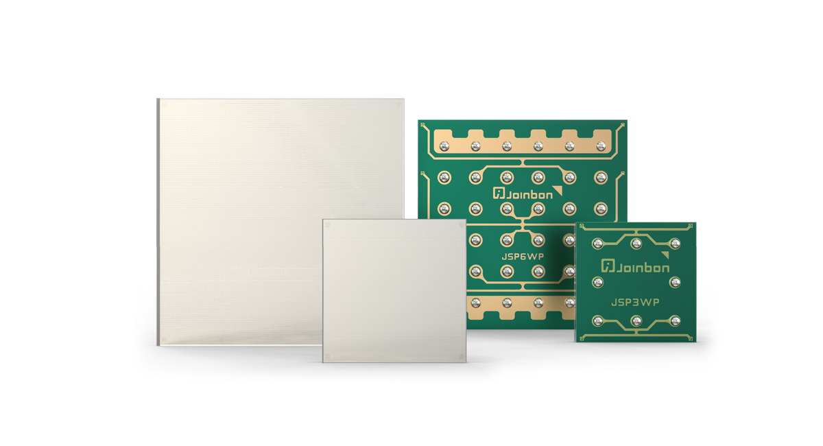
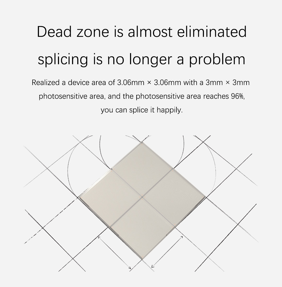
The photosensitive area accounts for up to 99%, the package size equals chip size is basically achieved, you can splice it happily


Based on advanced wafer level package, compactness and reliability

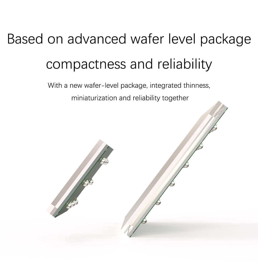
With a new wafer-level package, integrated thinness, miniaturization and reliability together


High-precision lithography signal path, with better uniformity and stability

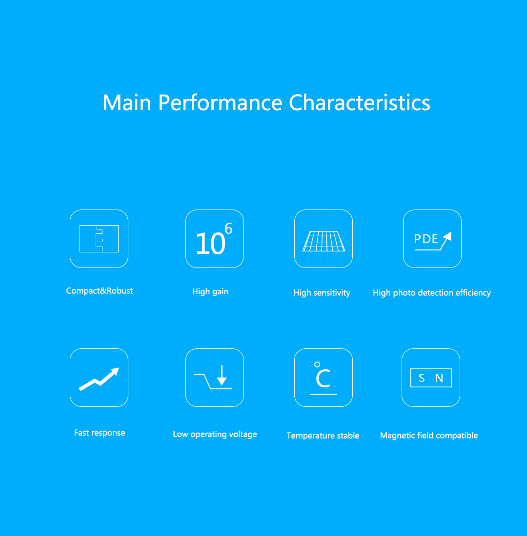
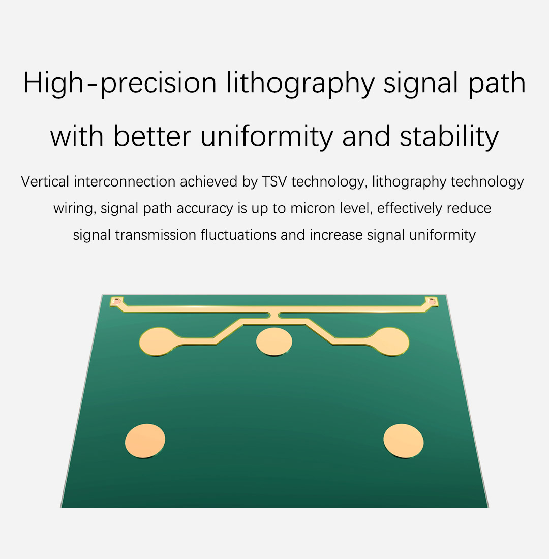
Vertical interconnection achieved by TSV technology, lithography technology wiring, signal path accuracy is up to micron level, effectively reduce signal transmission fluctuations and increase signal uniformity


High photon detection efficiency

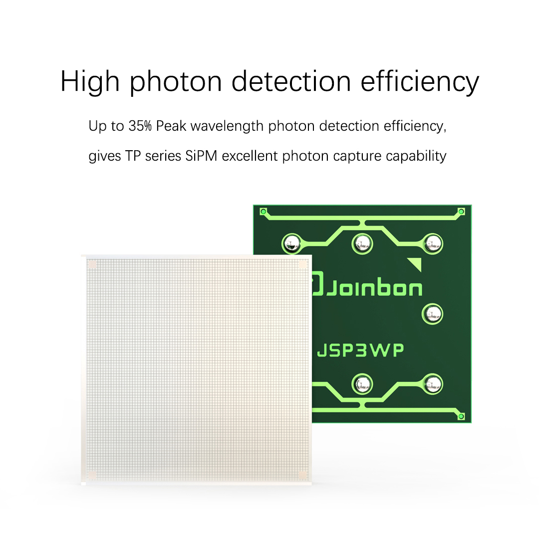
Up to 35% Peak wavelength photon detection efficiency, gives TP series SiPM excellent photon capture capability

Single photon sensitivity


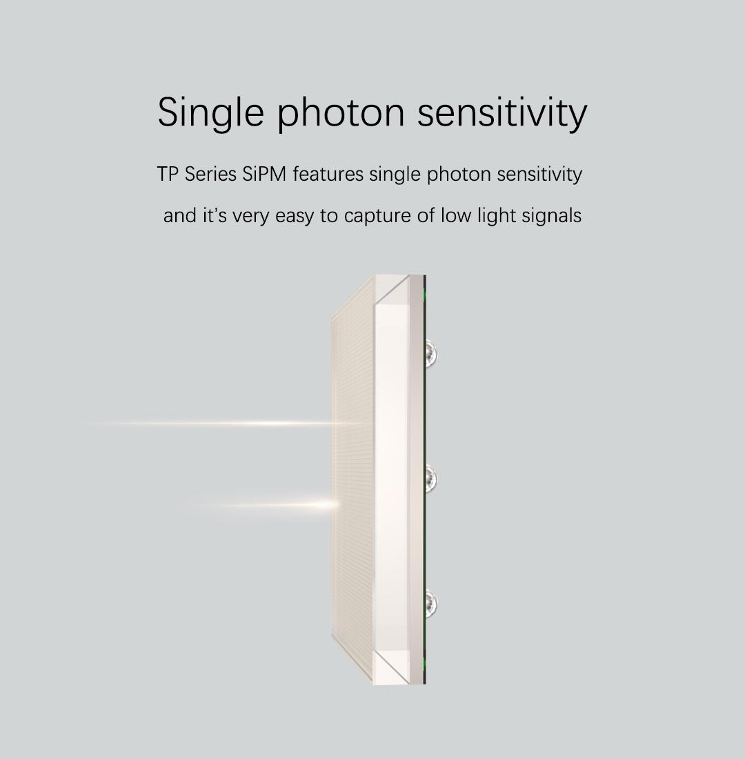
TP series SiPM features single photon sensitivity and it’s very easy to capture of low light signals

Excellent time performance


Ultra-fast response, signal rise time as low as 1ns

36mm2 photosensitive area, the best choice for

 large area detection


In the case of the same photosensitive area, the TP6000 series can significantly reduce the number of channels, making it easier to use,

and the cost per unit area is further reduced, which is more cost-optimized